
Conductive Inks for Smart and Sustainable Applications
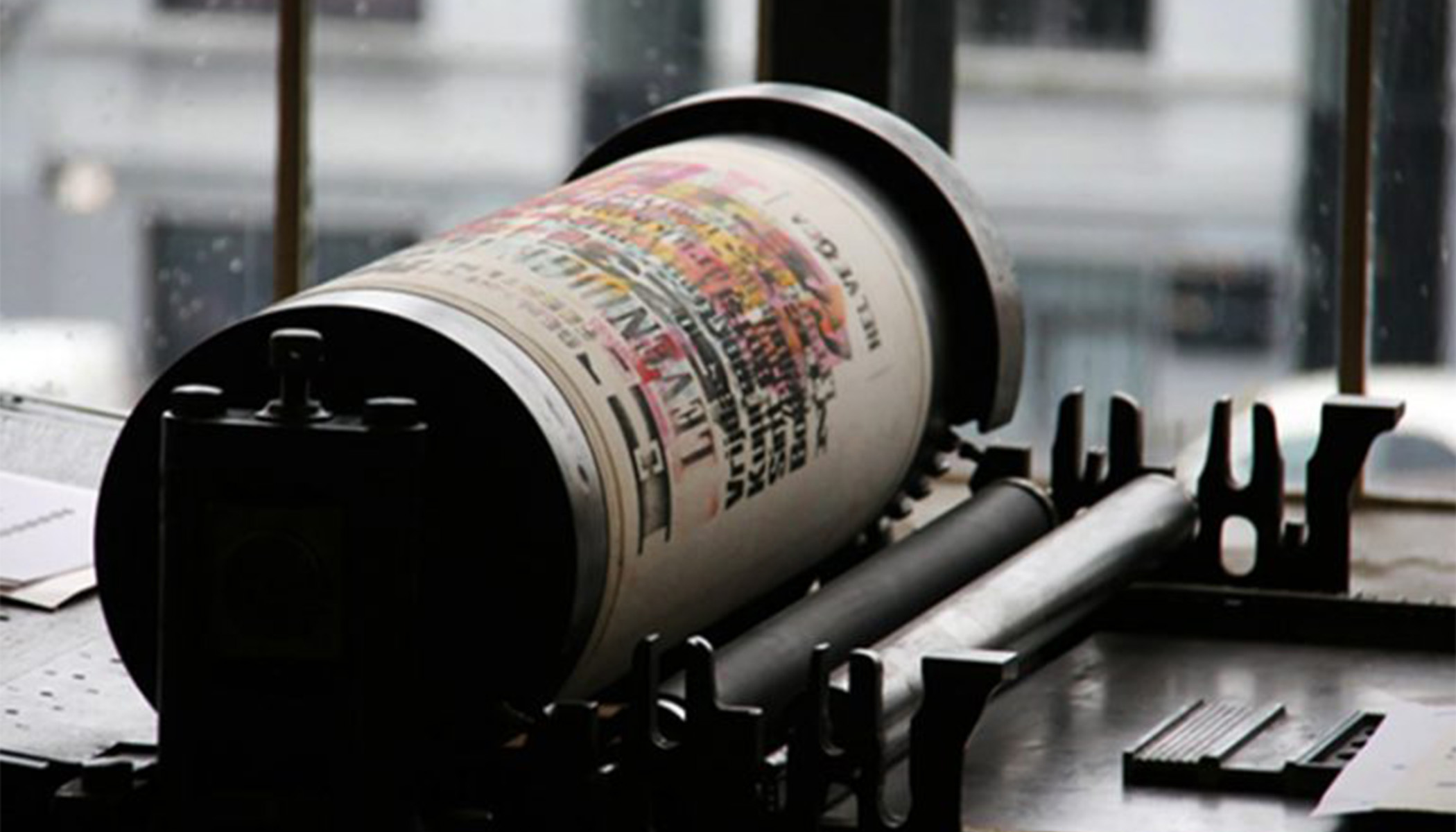
Printable electronics are a promising field of research whose technical development is focused on conductive-ink printing technologies appropriate for a wide range of support materials such as paper, plastic, or fabric.
Printable electronics have huge potential, and find application in flexible displays, sensors, solar cells, and wearable devices. However, it is still a technical challenge to achieve high electron mobility in printed conductive tracks, that is, the speed of electron movement through a material, which is an essential property for fast and efficient electronic performance.
Background
Many commercially available printable inks, such as silver, carbon, gold or copper polymer/solvent blends, have low electron mobility compared to silicon – the dominant material for conventional rigid electronics, leaving a need for new printable inks that can offer high electron mobility whilst retaining the compatibility with different printing methods on rigid and flexible substrates.
Researchers from the University of Cambridge have developed a novel method of ink production for roll-to-roll printing based on layered nanomaterials such as graphene. The remarkable properties of graphene include high electron mobility and electrical conductivity making them ideal for high-performance inks.
Technology overview
- The technology is a new, simple, scalable and effective method to exfoliate graphite into graphene in a controllable way.
- This works by shearing graphite under high pressure in a microfluidic channel to cause the exfoliation of graphite to graphene nanoplatelets and graphene with minimal to no chemical modification.
- Produced graphene nanoplatelets can be controlled in terms of lateral size and thickness and can be used to formulate highly conductive inks.
- The inks are attained by dispersing nanoplatelets in a carrier solution, and can go on to be screen printed to form conductive patterns on flexible or rigid substrates.
Benefits
- Highly dispersed graphene inks optimized for printing on rigid or flexible substrates
- Inks with high electrical and thermal conductivity.
- Method scalable to large volumes.
- Screen printable.
- High conductive particle loading available giving control over conductivity.
- Tailored electrical and optical properties depending on material (e.g. mobility>100cm2/V/s).
- Good optical and electrical homogeneity of deposited material (<10% std dev).
- Mechanical flexibility and environmental stability.
- Large scale deposition possible using full range of printing methods including inkjet printing.
- Suitable for printing of multiple layers.
Applications
- RFID tags
- Smart Packaging
- Conductive inks in vehicles
- Sensors (imaging, temperature, gas, glucose, force and strain, consumer electronics, skin patches)
- ITO replacement (touch screens)
Opportunity
We are seeking industrial experts and partners to commercialise the technology under license.
Inventors
This technology was developed at the Cambridge Graphene Centre (CGC). The mission of the CGC is to investigate the science and technology of graphene, carbon allotropes, layered crystals and hybrid nanomaterials. The CGC promotes innovative and adventurous research with an emphasis on applications by effectively establishing joint industrial-academic activities.
Cambridge Graphene Centre | Research Centre on Graphene, Layered Crystals and Hybrid Nanomaterials
References & Patents
EP3359611A1 – Layered materials and methods for their processing – pending
US10906814B2 – Layered materials and methods for their processing – granted
CN108473802B – Layered material and method for processing same – granted
JP6914251B2 – Layered material and its treatment method – granted