Just when it seemed that microchips couldn’t get any tinier, a technique developed by researchers at the University of Cambridge could lead to chips which are not only smaller, but can support electrical current densities five times greater than the current technology.
The technique, developed by Professor John Robertson and Santiago Esconjauregui of the University’s Department of Engineering, uses special arrangements of carbon atoms to carry electric current through the microchips.
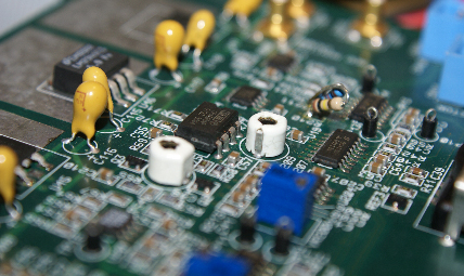
Microchips, also known as integrated circuits (ICs), are used in almost all electronic equipment, from computers to mobile phones to any number of the digital appliances found in the average household. Their small size and low production cost have revolutionised the consumer electronics industry.
Integrated circuits are constructed in layers, each with many separate electrical components that are connected together by tiny copper wires, both within and between the layers. As manufacturers attempt to make integrated circuits smaller and smaller, the copper connectors must become smaller too, and the electrical current density within the copper becomes proportionally higher, until eventually no more current can be passed through the copper connector.
Professor Robertson and his colleagues have devised a method using carbon nanotubes to replace the vertical copper connectors in ICs, allowing ever smaller circuits to be built, reducing the size of electronics even further.
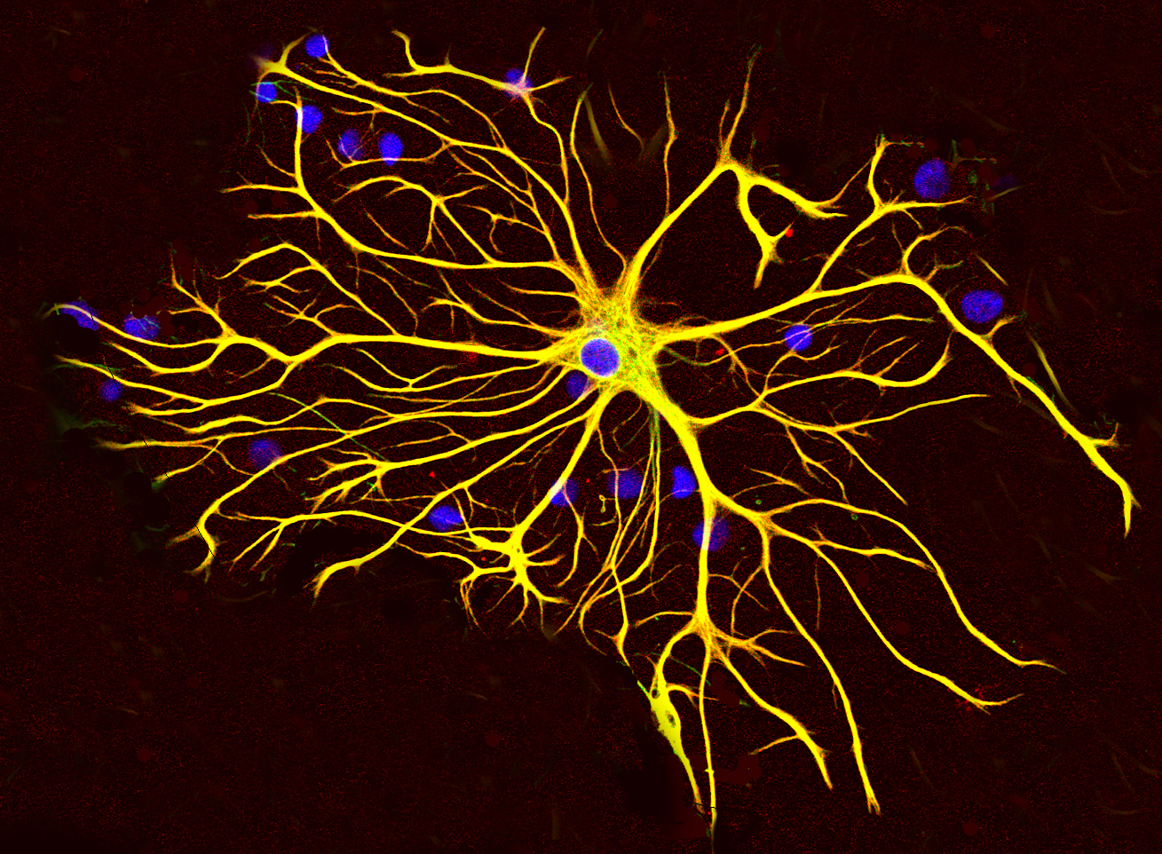
Carbon nanotubes consist of a special arrangement of carbon atoms. Normally, as in graphite, the atoms are arranged hexagonally and layered in sheets. In nanotubes however, the sheets are rolled up to form minute tubes, only a few atomic dimensions in diameter.
Individual carbon nanotubes can support extremely high electrical current densities, and are excellent candidates to replace copper to connect IC layers. However, in order for this to be feasible, the nanotubes need to be grown in very dense bundles directly onto the substrate.
Nanotube bundles are normally grown by depositing a thin film of catalyst, such as iron, onto the substrate and changing the properties of the catalyst through the use of heat, a process known as annealing. Annealing produces a series of nanoparticles which are the basis for the growth of each nanotube. This method does produce nanotube bundles, but they have limited spatial density, and carry insufficient electrical current for microchip purposes.
Professor Robertson and his colleagues have devised a method for growing nanotube bundles through multiple deposition and annealing steps, resulting in successive increases in nanoparticle density. The resulting bundles have a density that is five times greater than the closest available technology, with further density increases possible in the future.
Professor Robertson will present his research at the International Electron Devices Meeting of the Institute of Electrical and Electronics Engineers, which takes place from 6-8 December in San Francisco.
Electronics by Ward via Flickr